Note: Link for the multisim file needed for the simulation is provided at the end of the post.
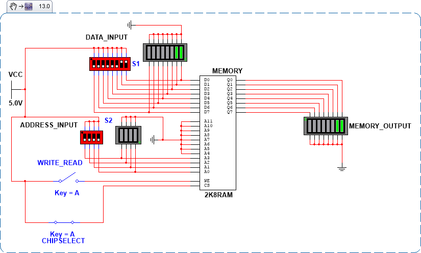
In this part we are going to simulate a RAM (Memory). The Memory shown below has 2k locations (words) each of size 8 bit. 8 bit word size implies a data input and data output of 8 bit denoted as D0-D7 and Q0-Q7 respectively. 2k memory locations implies an address line of 12 bit denoted as A0-A11. There’s a Write Enable (WE) input. The RAM (memory) performs a write operation when WE is high. It performs read operation when WE is low. There’s a Chip Select (CS) input which enables/disables the memory when it is high/low.
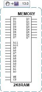
FIG 1 provides the circuit setup to simulate the Memory. There’s an 8 item dip switch pack connected to the data input (D0-D7). This switch helps us input data into the memory. There’s a 4 item dip switch pack connected to address input (A0-A3). Note that this setup let us input an address of only 4 bit. This means only 16 out of 2k locations are addressable.Switch is provided for WE and CS. LED outputs are provided so that the status of each section can be determined nicely.
How to Write and Read:
At first turn off the WE switch and turn on the CS switch. To write into the memory simply set the desired bit value in the 8 item dip switch pack connected to D0-D7. Then set the desired address by setting the bit value in the 4 item dip switch pack connected to A0-A3. Then, turn on the WE switch.
To read the data simply provide the desired address by setting the bit value in the 4 bit item dip switch pack connected to A0-A3 and turn off the WE switch.
To disable the Memory, turn off the CS switch.
Link for the multisim file
https://drive.google.com/folderview?id=0B8cy5TgcyxKMX29rUXNzOEp3cFU&usp=sharing
